This documents shows knowledge on the physics of microwave semiconductor devices and noise concepts. The term "pixel" in this document refers to a "pixel amplifier", which is D band horn antenna with a low noise HEMT (High Electron Mobility Transistor) based amplifier, hereafter called the "LNA".
Subject: On your client's email
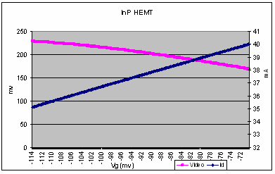
Graphically things become clearer:
There are a handful of objections to your client's comments
“Of course, the output voltage is directly proportional to drain current”
This leaves me with questions: The ambient temperature was stable, but was the pixel temperature kept constant during this measurement in which the power dissipation was increased in 33%? Does this experiment resemble in any way the thermal condition in which it will finally operate?
Channel temperature affects electron mobility and thus transconductance which translates into output video voltages. These devices exhibit channels down to 0.2 micrometers; all the quiescent power is dissipated right there, which is a very small volume and so they could be very sensitive to not having a good heat sink. This could be a possible explanation for the observed overall decrease in gain upon an Id increase. Also, Id is expected to go quadratic with Vg but the Id shows almost linear, in other words, Id is not incrementing at the expected rate, this could be explained by the effect of channel temperature as well.
Let’s get back to your client's email:
“This means that for every mV you move the gate, the output will move 1.39mV.”
This is a fair statement.
“The thermal sensitivity measured for this pixel was 0.129 mV/K.”
This is probably true.
“A mV gate change would cause a relatively enormous shift in the output”.
This calls for some serious stability in the gate voltages.
“It seems that some type of desensitizing circuit “
This I have no idea of what could mean…
“or increased precision of that DAC will be needed.”
In the original design, the range was set to go from +1.25 to – 1.25, with a ½ divider, it is going to be changed to a 1/20 divider rendering a LSB of 0.06 mV.
“Drain current changes with gate voltage at a rate of about 0.111mA/mV.”
So this means 6.66 micro amps per LSB. With the mentioned changes and the Id measurement that has an LSB of 14 micro amps, we could be controlling the drain current down to the +/-14 micro amps or +/-0.035% of the quiescent point Id current. Bias variations within a frame should be at least 10 times below these values. I think we are good with what we plan to have.
By the way, these measurements have helped me understand better the LNA. I wondered what could be the threshold voltage of the InP HEMT said to be used in the LNA. A piece of information like the threshold voltage says about how tight is our range for Vg.
Since the Id dependence on Vg is quadratic for all field effect transistors (HEMT devices are, after all the quantum stuff, field effect transistors too).
Id = K(Vg-Vt)2
Where Vt is the threshold voltage. Extrapolating the slope in the chart, the Id tangent will cut the Vg axis at -422 mv, meaning that Vt should be at -774 mv. I’ve seen reports that a 30% spread of Vt in HEMT devices is considered good. This means +/-116 mv. Our new span of +/-125 mv is relying on control over Vt being good.
Armando